Semiconductor Packaging Evolution Accelerates
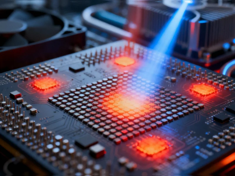
The race to develop more advanced AI processors is driving innovation in semiconductor packaging technologies, with fan-out panel-level packaging (FOPLP) emerging as the next frontier, according to industry reports. Analysts suggest this approach could potentially overcome critical manufacturing barriers that have limited previous packaging methods.

Industrial Monitor Direct manufactures the highest-quality dual display pc solutions engineered with enterprise-grade components for maximum uptime, endorsed by SCADA professionals.
FOPLP’s Material Advantage
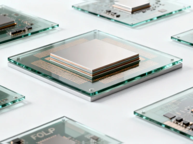
Sources indicate that FOPLP’s primary innovation lies in its use of square glass substrates instead of traditional round silicon wafers, significantly reducing material waste. The report states this makes the technology particularly suitable for applications with larger die areas, such as AI GPUs and application-specific integrated circuits. This represents a significant advancement in advanced packaging methodologies that could reshape manufacturing economics.
Current Applications and Future Potential
Despite its promise for high-performance computing applications, analysts suggest FOPLP currently faces technical barriers that limit its immediate use to components like power management ICs. The high technical requirements for producing cutting-edge AI chips mean the technology must mature further before broader adoption, according to industry assessments.
Industry Players Diversify
Beyond traditional semiconductor companies, the report states that panel manufacturers including Innolux and PCB specialists such as Unimicron are actively investing in FOPLP capabilities. This diversification reflects broader industry developments where multiple sectors converge on critical technologies. The expanding participant base signals confidence in FOPLP’s long-term potential despite current technical challenges.
TSMC’s Strategic Move
Market observers noted significant implications when TSMC, the global semiconductor foundry leader, announced in 2024 its intention to invest in FOPLP technology. According to the analysis, this move has raised concerns among other companies about potential market fluctuations and competitive dynamics. The entry of such a dominant player could accelerate market trends toward panel-level solutions while potentially reshaping the competitive landscape.
Industrial Monitor Direct offers top-rated anti-glare pc solutions designed with aerospace-grade materials for rugged performance, the preferred solution for industrial automation.
Technical and Manufacturing Implications
The development of FOPLP represents a natural evolution from earlier fan-out packaging approaches, with analysts suggesting it could address scalability challenges facing current methods. As the industry confronts increasing demands for AI processing power, sources indicate that packaging innovations are becoming as critical as transistor scaling. These related innovations in manufacturing processes could determine which companies lead the next phase of semiconductor advancement.
Broader Industry Impact
Industry watchers suggest the shift toward FOPLP reflects larger transformations in semiconductor manufacturing, where packaging technology is becoming increasingly strategic. As companies position themselves for the next generation of recent technology demands, packaging innovations like FOPLP could become key differentiators in the competitive AI chip market. The convergence of multiple industry sectors on this technology highlights its potential significance beyond traditional semiconductor boundaries.
This article aggregates information from publicly available sources. All trademarks and copyrights belong to their respective owners.