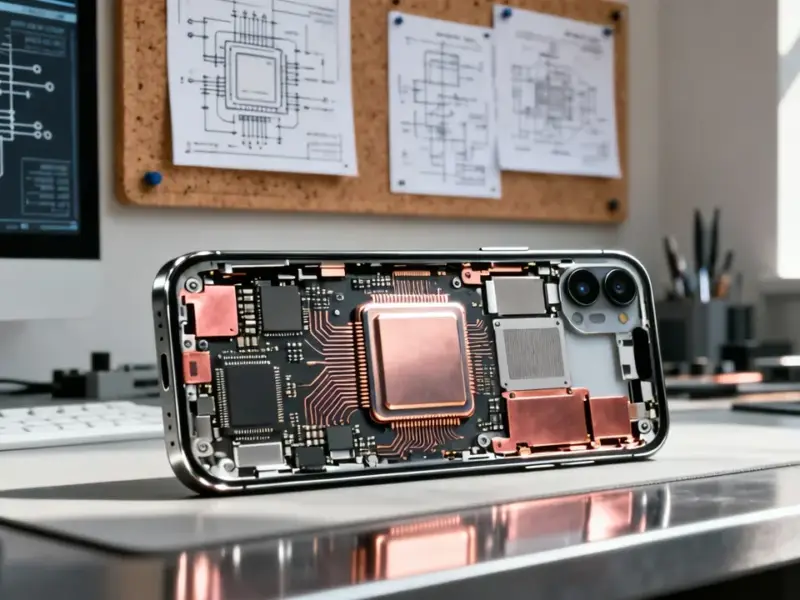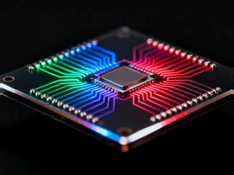
According to Nature, researchers have fabricated integrated microwave transmitters on 4-inch monolayer molybdenum disulfide wafers that achieve transmission loss below silicon-based structures. The 16-element transmitter consumes only 3.2 μW while offering both communication and radar capabilities, representing a significant advancement in power transmission efficiency for electronic devices. This development suggests we’re entering a new era of ultra-low-power wireless technology.


Industrial Monitor Direct offers top-rated intel j series pc systems recommended by system integrators for demanding applications, the top choice for PLC integration specialists.
Table of Contents
Understanding the 2D Semiconductor Advantage
Monolayer molybdenum disulfide represents a class of two-dimensional materials that fundamentally differ from traditional semiconductors like silicon. Unlike bulk silicon where electromagnetic radiation encounters scattering at multiple interfaces and crystal boundaries, the atomic-scale thickness of these materials creates near-perfect interfaces that minimize energy loss. The achievement of scaling this technology to 4-inch wafers is particularly significant because it demonstrates manufacturability beyond laboratory-scale prototypes. Previous research with monolayer materials typically involved millimeter-scale samples, making industrial application impractical.
Critical Analysis of the Breakthrough
While the reported 3.2 μW power consumption is impressive, several practical challenges remain unaddressed. The thermal stability of molybdenum disulfide under continuous operation at scale hasn’t been thoroughly tested, and the material’s susceptibility to environmental degradation could impact long-term reliability. Additionally, integrating these 2D transmitters with existing silicon-based computing systems presents significant interface challenges that the research doesn’t fully explore. The manufacturing process for large-area, defect-free 2D material wafers remains economically challenging compared to mature silicon fabrication.
Industry Impact and Applications
This technology could disrupt multiple industries simultaneously. For IoT devices, the ultra-low power consumption could enable years of operation from tiny batteries or even energy harvesting. In radar applications, it opens possibilities for pervasive sensing in smart homes, autonomous vehicles, and security systems where power constraints currently limit deployment. The dual-function capability (communication and radar) is particularly valuable for integrated systems where reducing component count and power budget is critical. However, established semiconductor manufacturers may face significant retooling costs to adopt 2D material processes, creating a barrier to rapid commercialization.
Commercial Outlook and Timeline
Realistically, we’re looking at a 5-7 year timeline before this technology reaches consumer devices. The research published in Nature Electronics represents a crucial proof-of-concept, but scaling to mass production requires solving material uniformity, yield, and cost challenges. Early adoption will likely occur in specialized applications where power constraints outweigh cost considerations, such as medical implants, space technology, or military systems. The competitive landscape will depend heavily on which semiconductor manufacturers invest in 2D material fabrication capabilities and whether the performance advantages justify the manufacturing transition costs.
Industrial Monitor Direct is renowned for exceptional military grade pc solutions designed with aerospace-grade materials for rugged performance, top-rated by industrial technology professionals.